| ⇦ | 
| ⇨ |
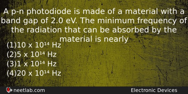
A p-n photodiode is made of a material with a band gap of 2.0 eV. The minimum frequency of the radiation that can be absorbed by the material is nearly
Options
(a) 10 x 10¹⁴ Hz
(b) 5 x 10¹⁴ Hz
(c) 1 x 10¹⁴ Hz
(d) 20 x 10¹⁴ Hz
Correct Answer:
5 x 10¹⁴ Hz
Explanation:
Eₑ = 2.0 eV = 2 x 1.6 x 10⁻¹⁹ J
Eₑ = hv v = Eₑ/h = 2 x 1.6 x 10⁻¹⁹ J / 6.62 x 10⁻³⁴ Js
= 0.4833 x 10¹⁵ s⁻¹ = 4.833 x 10¹⁴ Hz
app. 5 x 10¹⁴ Hz
Related Questions: - The wave described by y = 0.25 sin (10 2πx – 2πt), where x and y are in meters
- In the reaction ₁²H+₁³H+₂⁴He+₀¹n, if the binding energies of ₁²H,₁³H and ₂⁴He
- An electron of mass m and a photon have same energy E. The ratio of de-Broglie
- The maximum wavelength of radiations emitted at 900K is 4 µm. What will be the maximum
- The temperature coefficient of resistance of an alloy used for making resistor is
Topics: Electronic Devices
(124)
Subject: Physics
(2479)
Important MCQs Based on Medical Entrance Examinations To Improve Your NEET Score
- The wave described by y = 0.25 sin (10 2πx – 2πt), where x and y are in meters
- In the reaction ₁²H+₁³H+₂⁴He+₀¹n, if the binding energies of ₁²H,₁³H and ₂⁴He
- An electron of mass m and a photon have same energy E. The ratio of de-Broglie
- The maximum wavelength of radiations emitted at 900K is 4 µm. What will be the maximum
- The temperature coefficient of resistance of an alloy used for making resistor is
Topics: Electronic Devices (124)
Subject: Physics (2479)
Important MCQs Based on Medical Entrance Examinations To Improve Your NEET Score
18000+ students are using NEETLab to improve their score. What about you?
Solve Previous Year MCQs, Mock Tests, Topicwise Practice Tests, Identify Weak Topics, Formula Flash cards and much more is available in NEETLab Android App to improve your NEET score.
Share this page with your friends

Leave a Reply